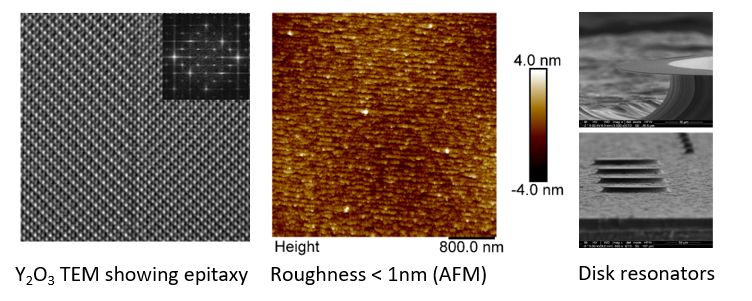
 Quantum networking is a vital branch of the next generation of quantum technology, necessary to enable the distribution of quantum information for applications such as distributed quantum computing, distributed quantum sensing, and quantum key distribution. One of our key interests is the development of scalable quantum memory devices for repeater-based quantum networks. Our platform of interest is erbium-doped thin film oxides, including TiO2, CeO2, CaWO4, and CaMoO4, grown (on silicon substrates) with our lab’s dedicated molecular beam epitaxy (MBE), atomic layer deposition (ALD), and sputter tools. We fabricate our devices using the extensive cleanrooms at Argonne and the University of Chicago, and the devices and structures are characterized using extensive in-house optical and spin property measurement capabilities that include measurements down to mK temperatures. Our focus here is applied research—to transition this activity from fundamental materials and physics measurements to compact and scalable photonic devices. Our research encompasses all stages of this development: materials growth, optical characterization, spin characterization, and design and fabrication of integrated nanophotonic devices. A startup, memQ, has emerged out of this research. Our program is primarily funded via QNEXT, one of the Department of Energy’s 5 National Quantum Science Research Institutes (NQSIs), where Professor Guha is the CTO.
Group Participants: Dr. Gregory Grant, Ignas Masiulionis, Sagar Kumar Seth, Claire McDermott, Jialun Ge, Yizhi Zhao
Collaborators: Dr. Jiefei Zhang, Dr. Alan Dibos, Dr. F. Joseph Heremans, Dr. Jianguo Wen, Dr. Swarnabha Chattaraj — Argonne National Lab; Prof. David Awschalom, Prof. Peter Maurer— UChicago
Funded via a Department of Energy program where Professor Guha is Principal Investigator, we are working on three classes of nanostructured materials that can collectively revolutionize computing memory if we are able to achieve precise, atomic-scale control of their dynamic behavior. These are: scale-free ferroelectrics and spin memories (on-chip); and a new optically addressed atomic memory (off-chip). Such memory will be non-volatile, fast, analog-to-multibit tunable, up to 1000× denser than today’s, and applicable across many architectures, from embedded to neuromorphic. We are working on unveiling the underlying science to establish this control and materials processes for building the heterostructures and quantifying system impact. Techniques include synthesis, ultrafast electron and X-ray microscopy, exascale atomic simulations of full devices, and atoms-to-systems codesign that rethinks how computing, thus reinforced, is reshaped. For this we are working as part of a multidisciplinary team from Argonne, UChicago, Chicago State U, Purdue, Georgia Tech, and industry collaborators from IBM and Micron.
For ferroelectric memories, we are pursuing scale-free properties centered around hafnia and related alloys--exploring the atomistic limits of cell localization, the pathways and dynamics of polarization reversal, and the impacts of physical/chemical nanostructuring, based upon promising work from our team. New heavy-metal SOT sources with high spin Hall coefficient and conductivity, perpendicularly-magnetized synthetic antiferromagnetic free layers with high interlayer coupling/low pinning, and nanometer precise current driven steering of magnetic domains are being studied in service of a new domain wall motion controlled multi-bit spin memory we have proposed. For volumetric storage-class memories, we are pursuing a new, theoretically backed approach, where we will “write” and “read” bits into single rare earth (RE) atom-trap pairs distributed in a RE doped solid host by exploiting the narrow homogeneous optical linewidths of 4f transitions in REs. In-operando voltage triggered ultrafast electron microscopy (UEM) and high brightness coherent X-ray analysis; high speed electrical and magnetic measurements, and extensive thin film synthesis studies are being carried out to set a firm scientific foundation for these materials, enabling the atomistic level control necessary to make them useful.
Group Participants: Eeshan Ketkar, Dr. Wilfried Haensch, Dr. Pengxiang Zhang, Dr. Koichi Tanaka
Collaborators: Professor Giulia Galli, Dr. Swarnabha Chattaraj, Dr. Jiefei Zhang—U Chicago; Dr. CD Phatak, Dr. Dillon Fong, Dr. Subramanian Sankaranarayanan, Dr. Christopher J. Knight, Dr. Daniel Durham—Argonne; Professor Kaushik Roy and Professor Anand Raghunathan—Purdue University; Professor John (Archie) Peters--Chicago State University; Professor Suman Datta—Georgia Tech
The transition to quantum technologies, high-power microelectronic, and certain on-chip photonics technologies have increasingly relied on the maturation of hard/ultrahard, wide-bandgap oxides and semiconductors such as SiC, diamond, LiNbO3, yttrium iron garnet (YIG) etc. Manufacturing with these ultrahard and expensive materials presents significant challenges, particularly in wafer cost and integration.Additionally it is often desirable to heterogeneously integrate these materials with other materials and devices (such as silicon) for new functionality in devices and sub-systems. Our lab has developed a platform technology that enables controlled spalling and layer transfer of ultrahard wide-bandgap materials, allowing the removal of bulk-quality films that can be heterogeneously integrated onto other platforms. Using a nickel (Ni) stressor layer, we achieve thickness-controlled spalling of wafers to produce a few microns thick films. We have also developed a crack initiation method to deterministically control spalling direction. This approach has been successfully demonstrated on 4H-SiC, diamond, and YIG wafers, and their device characteristics have been studied for example, in qubit performance (SiC), and microwave-magnon coupling (YIG). A startup company, K1 Semiconductor, has emerged recently from this work.
Group Participants: Connor Horn, Sagar Kumar Seth
Collaborators: Prof. David Awschalom—U Chicago; Dr. Joe Heremans—Argonne National Lab; Prof. Xufeng Zhang—Northeastern University
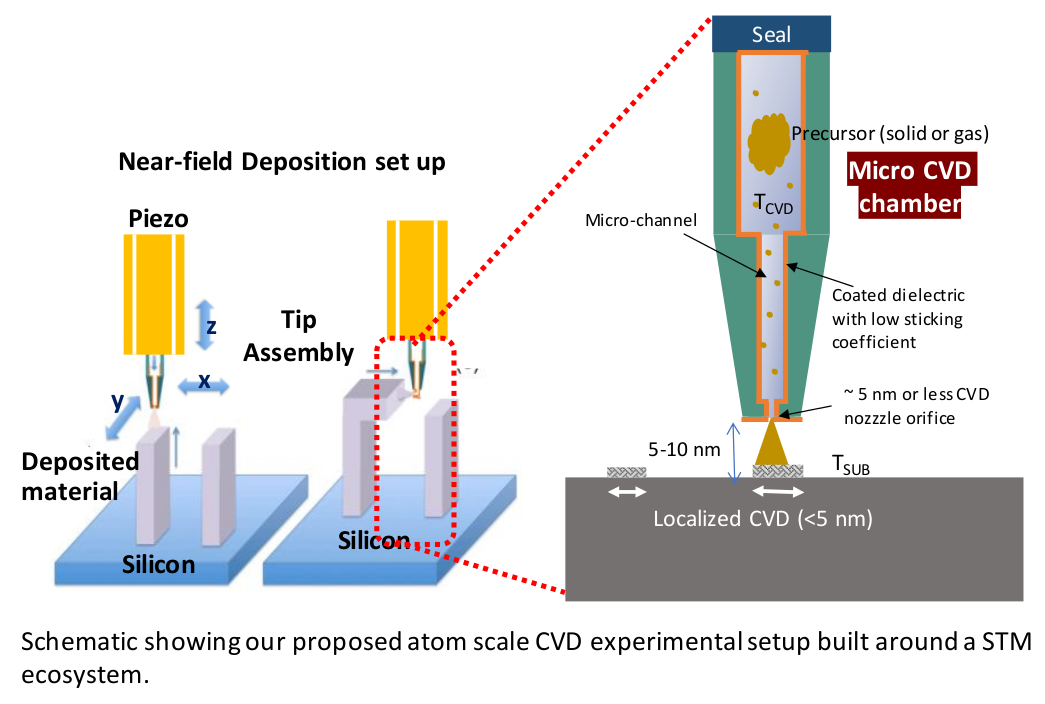 We are developing a gas-phase direct-write deposition system which performs additive patterning of physical vapor deposition (PVD), chemical vapor deposition (CVD), and atomic layer deposition (ALD) thin films directly onto arbitrary substrates, with no intermediate processing steps and with targeted microns to nanometer resolution. By coupling meso to nanoscale apertures (100um down to ~1nm, made from either silicon or quartz) with refined 3D scanning probe techniques, the aim of this project is to overcome the limitations of traditional lithography-based nanofabrication. Gas-phase direct-write has the potential for record-breaking additive patterning resolution, high thin film purity, patterning on organic or delicate substrates, natively 3D fabrication processes, and more. This research is currently focused on two main goals: (1) Exploring the ultimate resolution of gas-phase direct-write and understanding the fundamental limitations of this system—this leads to atom scale “direct write” and asks the question: can we deterministically deposit a single or few molecules at a time in a scalable fashion? This approach has applications in quantum information science and engineering and device fabrication at extreme size limits in microelectronics. (2) Developing methods for micron-scale “direct-write” features in three-dimensions at high deposition rates. This is applicable in areas such as heterogeneous integration for microelectronics. Our research also involves studying the mechanisms of crystal growth under such circumstances of a localized evaporant source at the near field of the substrate; and the design/testing of devices built using direct write.
Group participants: Xella Doi, Eeshan Ketkar, Dr. Koichi Tanaka
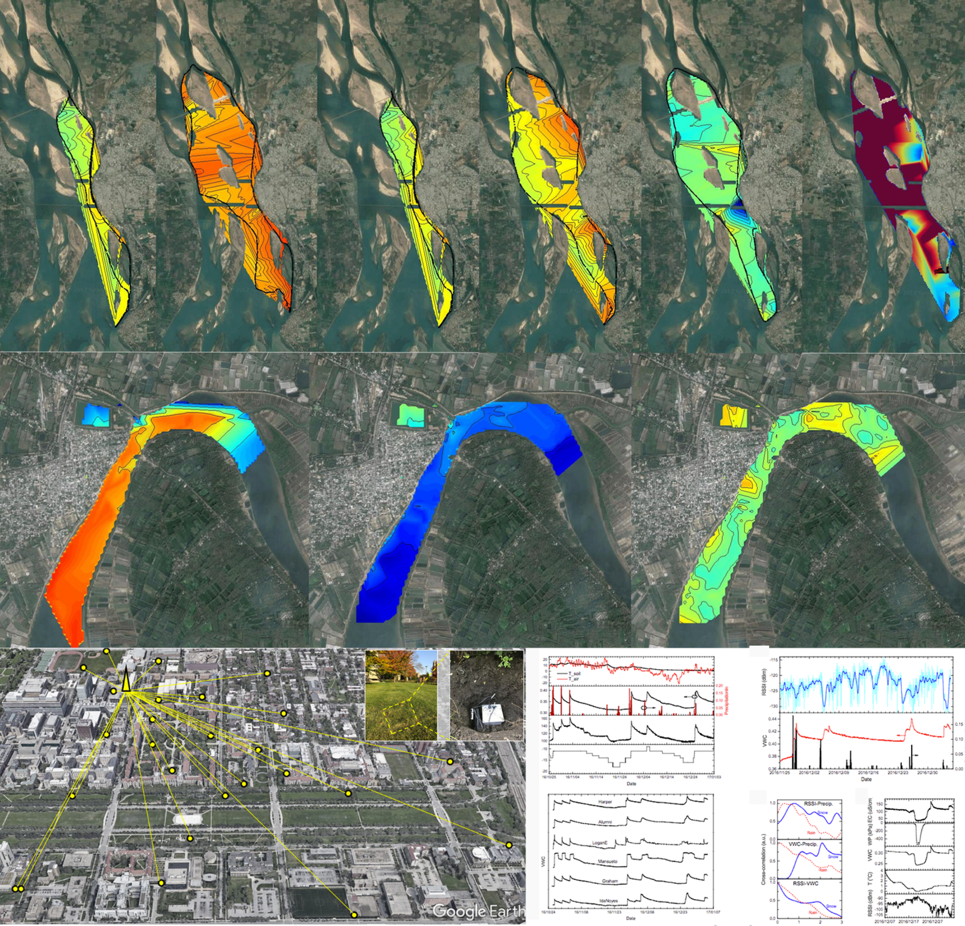 In a separate thread from the Guha Group’s core research on materials and devices, members of the team have been involved in a long term project on using geospatial sensor networks for water quality monitoring and terrestrial ecology. This research has spanned the measurement of rivers in India using mobile sensor platforms that measure a multitude of water quality paramenters, and building a buried wireless sensor network in working agricultural fields in Illinois for measuring parameters such as soil moisture. The objective of the project is environmental management. This work is multidisciplinary in nature and has developed in strong collaborations with Professor Anup Malani at the Harris School for Public Policy University of Chicago, with Dr. Roser Matamala a terrestrial ecologist at Argonne National Labs, and Professor Monisha Ghosh, a wireless communications expert at the University of Notre Dame. Currently, Dr. Srinivasa Balivada, a member of Dr. Guha’s team in India leads a project on the measurement and quantification of chlorine treatment management in a pilot project for delivering drinking water via tap to a group of India villages in the states of Odisha and Andhra Pradesh. This project is being done in collaboration with the Development India Laboratory led by Professor Michael Kremer of the Economics Department University of Chicago.